

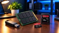
You probably touched flash memory a dozen times today without thinking about it once. The photos on your phone sit on it. The SSD inside your laptop is built from it.
That USB stick in your drawer, the SD card in your camera, the chip that wakes your motherboard up before Windows even loads, all of it is flash memory.
In 2026, the same technology serves two very different worlds. On one side, consumer gear keeps getting roomier and cheaper.
On the other, data centres now lean on flash for AI workloads, database servers and storage arrays that never sleep. Same core idea, wildly different demands placed on it.
If you want to buy storage for a business, or you're just tired of guessing which SSD is worth the money, you are in the right place.
What Does Flash Memory Mean?
Flash memory is non-volatile storage built from silicon chips. Non-volatile means the data stays put when the power goes off.
Pull a USB drive out mid-song and the file is still sitting there tomorrow. That single property separates flash memory from RAM (Random Access Memory), which wipes itself clean the second your machine loses power.
There are no moving parts anywhere inside it. No spinning platter, no read arm, no motor. Everything happens electrically within the chip, which is why solid-state drives survive drops that would kill a hard disk.
Flash grew out of EEPROM, short for electrically erasable programmable read-only memory. EEPROM could erase and rewrite data one byte at a time, which was painfully slow for anything large.
Flash rewrote the rules by erasing whole blocks at once. The name came from a Toshiba engineer who said the erase process reminded him of a camera flash, and it stuck.
How Flash Memory Stores and Erases Data
Inside every flash chip sit millions of floating-gate transistors. Picture each one as a tiny sealed jar wrapped in insulation. Push electrons into the jar and the cell reads as one value.
Leave it empty, and it reads as another. The insulation traps those electrons when the power is gone, and that's the whole trick behind non-volatile storage.
Three operations happen on those cells, and each one behaves differently:
Read: The chip measures the voltage in a cell to work out what's stored. Reading is fast and does no damage to the cell.
Write (program): Electrons get forced through the insulation into the floating gate. Data goes in one page at a time.
Erase: Electrons get pulled back out. This one can't be done cell by cell. It happens across an entire block.
Block-level erasure is the part that catches people out. Flash can't simply overwrite old data the way EEPROM could byte by byte. The block has to be cleared first, then written fresh.
Controllers work around this by writing new data to empty pages elsewhere and marking the old pages as junk, then tidying up later during garbage collection.
Every one of those erase-and-write trips wears the insulation down a fraction. Do it enough times, and the cell stops holding charge reliably. That's why drives ship with endurance ratings, measured in program/erase (P/E) cycles or terabytes written (TBW).
Wear levelling is the counter to that problem. The controller spreads writes evenly across every available block instead of hammering the same few, so no single patch of the chip burns out while the rest stays fresh.
NAND vs NOR Flash Memory
Both are flash memory. The difference lies in how the cells are wired together, and that wiring decides what each one is good at.
NOR Flash: Built for Code, Not Capacity
NOR flash connects its memory cells in parallel, with each cell wired so the processor can reach it directly. That gives you random byte access. The chip can pull any single byte without reading through everything sitting in front of it.
That matters for code. A processor can run instructions straight out of NOR flash without copying them into RAM first, a trick called Execute in Place (XIP).
It's why NOR sits in BIOS and UEFI chips, microcontrollers, industrial firmware, and automotive control units. When your PC boots, the very first code it runs comes out of NOR flash.
The catch is space. All that parallel wiring eats die area, so NOR holds far less data per chip and costs much more per gigabyte. Intel brought NOR flash to market in 1988 as the first commercial flash format, and it still owns the code-storage job today.
NAND Flash: Built for Storage, Not Code
NAND flash strings its cells in series, commonly eight or more transistors sharing a single connection. Fewer wires per cell means far more cells packed into the same silicon area.
That density is the entire point of NAND. It holds much more capacity at a fraction of the cost per gigabyte, which is how it ended up inside every USB drive, SSD, SD card, and phone on the market.
The trade-off is access. NAND reads and writes in pages and erases in blocks, so it can't hand the processor a single byte on demand.
Code doesn't run directly from it. Toshiba introduced NAND in 1989, one year after NOR, aimed squarely at high-density data storage. That split still holds: NOR for code, NAND for files.
Cell Types Inside NAND Flash: SLC, MLC, TLC and QLC
A NAND cell doesn't have to hold just one bit. Squeeze more voltage levels into the same cell, and you store more data in the same physical space.
The price you pay is precision. More levels crammed in means narrower gaps between them, slower reads, and quicker wear.
Single-Level Cell (SLC): One Bit, Maximum Endurance
SLC stores one bit per cell, so the chip only has to tell two voltage states apart: charged or not charged.
That wide margin makes it the toughest and quickest NAND there is, rated in the region of 50,000 to 100,000 P/E cycles per cell.
You'll find SLC in industrial controllers, medical equipment, aerospace systems, network hardware, and write-heavy enterprise storage.
It costs the most per gigabyte by a wide margin, which only adds up when downtime or lost data costs more than the drive itself.
MLC (Multi-Level Cell): Two Bits, Better Value
MLC holds two bits per cell using four voltage states. Endurance lands somewhere around 3,000 to 10,000 cycles, well under SLC but comfortably ahead of TLC.
Reads and writes run a touch slower because the controller has to separate four levels instead of two. MLC suits higher-end consumer SSDs, workstation drives, and business machines with steady daily writes.
Its price sits in the middle, which makes it the sensible step down for buyers who want durability without paying industrial rates.
TLC (Triple-Level Cell): Three Bits, the Consumer Standard
TLC packs three bits per cell across eight voltage states, and it's what most people buy in 2026 without realising it.
Endurance runs roughly 500 to 3,000 cycles, which covers normal laptop, desktop, and office work for years.
The payoff is capacity. More bits per cell means more gigabytes per chip, and that's how 2TB and 4TB consumer SSDs became affordable.
For business use, TLC handles read-heavy jobs well: file servers, application hosts, virtual desktops. It's a poor match for database logging or anything writing to disk around the clock.
QLC (Quad-Level Cell): Four Bits, Maximum Density
QLC stores four bits per cell across sixteen voltage states, the densest option in production right now. It's the reason multi-terabyte drives keep dropping in price.
Endurance is the weak spot, commonly landing in the few-hundred-cycle range, and sustained writing wears it down faster than any other cell type.
Sequential write speed also falls off sharply once the drive's fast cache fills up.
QLC earns its place in archives, backup targets, media libraries, and bulk storage where data gets written once and read many times over. If your workload writes hard every single day, put it on TLC or better and leave QLC for the cold data.
|
Cell type |
Bits per cell |
Voltage states |
Endurance |
Best fit |
|
SLC |
1 |
2 |
Highest |
Industrial, medical, write-heavy enterprise |
|
MLC |
2 |
4 |
High |
Prosumer SSDs, business workstations |
|
TLC |
3 |
8 |
Moderate |
Laptops, desktops, read-heavy business use |
|
QLC |
4 |
16 |
Lowest |
Archives, backups, bulk read-heavy storage |
Flash memory is one branch of a much larger family. If you want the full picture of how RAM, ROM, cache, and flash storage fit together, plus what to check before you fit any module into a machine, read our Ultimate Memory Guide 2026: Memory Type and Installation Precautions
Conclusion
Flash memory is non-volatile, solid-state storage that holds your data without power and has no moving parts to wear out mechanically.
NAND and NOR flash split the work between them: NOR for code that has to run in place, NAND for the bulk storage inside almost everything you own. Within NAND, the jump from SLC through QLC is a straight trade-off of endurance for density.
Knowing which cell type sits inside a drive changes how you buy. Two SSDs with matching capacity and similar price tags can have completely different working lives once you look past the label on the box.
In 2026, that picture is settled. NAND runs mass storage, NOR keeps firmware and embedded code alive, and 3D NAND stacking, now past 300 layers in volume production, is the standard route to more capacity without shrinking cells any further.
CTS Point stocks flash memory (RAM) products across both sides of that line, for people building a single machine and for businesses specifying storage at scale.
Browse our flash memory category, or get in touch and tell us what your workload looks like. We'll point you to the cell type that actually fits it.
Frequently Asked Questions
A: That question compares a material with a finished product. An SSD is built from NAND flash memory, so an SSD is flash memory housed in a drive with a controller and an interface attached. A single flash chip inside a phone isn't faster than an SSD. The SSD wins in practice because its controller runs many flash chips in parallel. What really moves the speed needle is the interface (SATA against NVMe), the controller quality, and the cell type, not flash against SSD.
A: Yes, and the gap gets wide. Two drives listing the same capacity can use different NAND grades, different controllers, different amounts of DRAM cache, and different firmware. Some budget drives even swap internal components partway through a production run while keeping the same model number. Check the controller, the cell type, and the TBW rating instead of trusting the capacity figure alone.
A: Flash has no seek time, so reaching any block takes about the same time no matter where it sits on the chip. That's why an SSD opens files far quicker than a hard drive. Within flash itself, reads are fastest, writes are slower, and erases are slowest by a long way. Once a drive fills up and free blocks run short, the controller spends more time clearing space before it can write, and write speed drops noticeably.
A: No. They all rely on NAND flash, but cell type, controller quality, and interface vary enormously. A cheap USB stick might use QLC with a basic controller and almost no error correction. A quality drive uses TLC with proper wear levelling and stronger error correction. Same shape and same connector, very different lifespan and speed.
A: Limited write endurance. Every erase and write cycle wears the cell insulation slightly, and each cell has a finite number of cycles before it stops holding charge reliably. Wear levelling stretches that life out, but it can't remove the ceiling. Flash also holds data as trapped charge, which leaks slowly over years of unpowered storage, so it isn't the right medium for archives you shelve and forget for a decade.
A: Yes. CTS Point supplies flash memory for both consumer and business setups, including higher-endurance options for write-heavy environments and high-capacity drives for archives and read-heavy work. Tell us what the workload looks like, and we'll match the cell type, capacity, and endurance rating to it.